
The method that sees without touching
A team of researchers has published an innovative method to observe what happens inside semiconductor chips in operation, without powering them down, disassembling them, or even touching them. The technique is based on coherent X-ray microscopy — specifically computational ptychography — and its implications reach well beyond the electronics industry. The same physical principles are being adapted for medical imaging detectors and for nondestructive analysis of implantable devices.
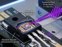
Modern chips are miniaturization marvels. A current commercial processor stacks dozens of layers of copper, insulator, and doped silicon, with transistors down to 3 nm feature size. Inspecting the internal integrity of those structures has traditionally required destructive delayering — cutting, polishing, and analyzing one slice at a time. The new method skips the entire chain: it uses X-ray diffraction and computational reconstruction to generate volumetric imagery of the device in operation.
How X-ray ptychography works
Ptychography (from the Greek ptychos, “to fold”) is a coherent imaging technique in which the object is illuminated by a focused beam and stepped in small overlapping increments. Each position generates a diffraction pattern that is captured by a pixelated detector. Iterative algorithms — typically based on the extended ptychographic iterative engine (ePIE) — combine those hundreds of patterns to reconstruct the object’s internal structure at a few-nanometer resolution.
The 3D version, known as X-ray ptychographic computed tomography (PXCT), adds object rotation during acquisition, enabling tomographic reconstruction. The result: volumetric maps with sub-100 nm resolution, capable of visualizing copper interconnects, transistors, and even silicon doping without destroying the chip.
What changes when the chip is powered
The recent leap is the ability to image chips in active operation — current flowing, transistors switching, heat dissipating. Imaging powered-off chips has been possible for some years (with the Paul Scherrer Institute in Switzerland leading the way). But the dynamic version lets engineers correlate physical structure with functionality — identifying which interconnect is heating up, where electromigration is happening, or where solder failures only appear under real-load conditions.
For the chip industry, that solves a long-standing problem: failure analysis in production. Today, when a chip lot fails, engineers must destroy units to understand what happened — losing unrecoverable evidence. With in-operation PXCT, diagnosis is possible without destruction.
Why this matters for medical imaging
A clinical reader may wonder: why cover this news on a radiology portal? The answer has three layers:
- Shared detectors: the pixelated X-ray detectors used in ptychography are direct cousins of the flat-panel arrays that equip digital radiography, tomosynthesis, and fluoroscopy. Advances in sensitivity, temporal resolution, and signal-to-noise ratio leak between the two industries. The IGZO bet for battery inspection illustrates that convergence.
- Reconstruction algorithms: the iterative methods that reconstruct ptychography are close relatives of iterative reconstruction in CT. Every algorithmic advance on one side tends to inspire the other — and scanner manufacturers are paying attention.
- Implant analysis: coronary stents, implantable electronic devices (pacemakers, neurostimulators, CGMs) can be analyzed with similar techniques to detect fatigue and failure without explanting. Medical device companies already contract synchrotron beam lines for that purpose.
Practical limitations
Before imagining PXCT in the clinic, recall its limits. First, the method needs a highly coherent X-ray source — typically a synchrotron or a free-electron laser. These are $100 million to $1 billion facilities, installed at national labs (SLAC, PSI, Diamond, Sirius in Brazil). This is not a technology that drops into a medical office.
Second, acquisition times are long — minutes to hours per sample, depending on target resolution. For a stationary semiconductor chip, that is acceptable. For a human patient, clearly not. Adapting the technique for clinical applications will require compact coherent X-ray sources, still in development.
The link to industrial radiology
For radiologists and medical imaging professionals, the news is a reminder: the frontier of X-ray physics keeps moving fast, and every advance over there reverberates in our field. Better detectors, more sophisticated reconstruction algorithms, brighter sources — all of that eventually makes its way into the medical scanner market.
Brazil’s Sirius synchrotron in Campinas offers world-class infrastructure for ptychography and related techniques. Brazilian groups have been publishing relevant work in chip metrology, materials, and biomaterials. That technical ecosystem forms the base for the next generation of medical detectors to include national contributions — not just as buyers but as protagonists.
One last thought worth keeping in mind: imaging history has been a story of cross-pollination. X-ray crystallography fed structural biology; computed tomography learned from radar; MRI borrowed from NMR spectroscopy. The current generation of coherent X-ray imaging may be doing the same for the next generation of clinical scanners — and the engineers behind today’s chip-inspection breakthroughs are quietly building tomorrow’s medical imaging toolkit.
Source: Inovação Tecnológica — X-ray vision sees inside operating chips